


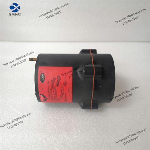
AMAT 0090-07135: Technical Specifications
- Component Type
- Category: RF (Radio Frequency) Matching Network or Plasma Source Component
- Purpose: Optimizes RF power delivery to sustain stable plasma during etching or deposition processes.
- Material: High-frequency ceramic insulators (e.g., Al₂O₃) and corrosion-resistant metal alloys (e.g., anodized aluminum).
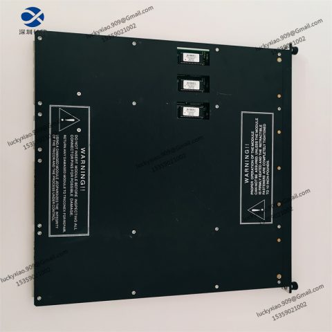
- Physical Specifications
- Dimensions: Modular design (approx. 300 mm x 200 mm x 100 mm) for integration into cluster tools.
- Weight: 5–8 kg (dependent on cooling system integration).
- Electrical & Operational Parameters
- Frequency Range: 2–60 MHz (adjustable for impedance matching).
- Power Handling: Up to 5 kW continuous RF power (peak power tolerance: 8 kW).
- Impedance Matching: Auto-tuning capability to maintain VSWR (Voltage Standing Wave Ratio) <1.5:1.
- Cooling System: Liquid-cooled (deionized water or glycol) to manage thermal load.
- Environmental Compatibility
- Vacuum Compatibility: Operates in high-vacuum environments (base pressure ≤ 10⁻⁶ Torr).
- Temperature Range: -20°C to 150°C (operational); up to 300°C short-term exposure.
- Integration & Interfaces
- Tool Platforms: Compatible with AMAT Centura® or Versa® etch/deposition systems.
- Control Interface: Digital communication protocols (e.g., SECS/GEM, Ethernet/IP) for real-time process monitoring.
- Certifications & Standards
- Complies with SEMI S2/S8 (safety and ergonomic standards).
- CE/UL certified for electrical safety.
- Lifetime & Maintenance
- Service Life: ~15,000–20,000 process hours (varies with plasma intensity and thermal cycling).
- Maintenance: Quarterly inspections recommended (e.g., capacitor health, coolant purity).
Functional Overview
The AMAT 0090-07135 is critical for advanced plasma-based processes in semiconductor manufacturing, ensuring high process stability and uniformity. Key functionalities include:
- Plasma Stabilization
- Automatically adjusts RF power delivery to maintain consistent plasma density, essential for uniform etching (e.g., anisotropic silicon etch) or deposition (PECVD).
- Minimizes arcing and process drift, reducing wafer defects.
- Impedance Matching
- Real-time impedance tuning compensates for load variations caused by chamber conditions or wafer materials (e.g., low-k dielectrics, copper interconnects).
- High-Power Efficiency
- Enables high-throughput processing with minimal energy loss, critical for 3D NAND or advanced logic nodes (3nm/2nm).
- Process Flexibility
- Supports both low-frequency (bias control) and high-frequency (plasma generation) regimes for multi-step processes.
- Applications
- Etch Processes: Deep silicon etch (TSV), dielectric etch (SiO₂, Si₃N₄).
- Deposition Processes: PECVD of SiO₂, SiN, or low-k films.
- Chamber Cleaning: NF₃/O₂ plasma cleans.
-480x480.png)
There are no reviews yet.