


_副本")
_副本")
_副本")
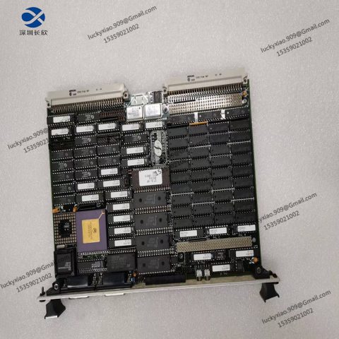
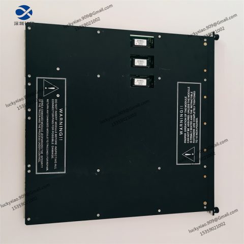
ASML MC1AB37 4022.437.1856 Product Introduction
ASML MC1AB37 4022.437.1856 is a dedicated high-precision motion control module engineered exclusively for ASML lithography systems. Built to meet the ultra-strict requirements of semiconductor cleanroom manufacturing, this module delivers closed-loop motion control for wafer and photomask positioning systems, enabling nanoscale alignment accuracy throughout the photolithography process. It features robust anti-interference circuitry and stable operational performance, adapting seamlessly to the demanding operating conditions of advanced chip production lines. Designed for long-term uninterrupted industrial use, it boosts manufacturing stability and yield while maintaining consistent precision for high-volume semiconductor production.
ASML MC1AB37 4022.437.1856 Technical Specifications
-
Product Model: MC1AB37, Part Number 4022.437.1856
-
Product Type: Precision Motion Control Module for Lithography Systems
-
Core Application: Closed-loop wafer & photomask alignment, precision motion actuation
-
Positioning Accuracy: Nanoscale precision for advanced semiconductor lithography
-
Operating Environment: Compatible with Class 100 semiconductor cleanrooms
-
Performance Traits: High-speed response, ultra-low drift, strong EMI resistance
-
Compatibility: Fully compatible with mainstream ASML lithography platforms
-
Design Standard: Industrial-grade rugged build for 24/7 continuous operation
-
Installation: Plug-and-play chassis-mounted design for straightforward integration
Recommended ASML Same-Series Models
-
4022.436.6099: Delivers stable power amplification for lithography motion components
-
4022.436.4154: Handles signal transmission and core control logic execution
-
4022.436.4163: Specialized PCB for precision signal conditioning & processing
-
4022.437.0198: Supports steady operation of high-performance motion systems
-
4022.456.07242: Manages wafer stage fixing and high-precision positioning
-
4022.471.7312: Provides regulated power supply for lithography system modules
-
4022.634.0601: Multi-axis synchronous motion control for complex lithography movements
-
4022.430.0325: Supports precision mechanical drive and feedback monitoring
-
4022.455.8921: Optimized for high-precision alignment in advanced EUV lithography
-480x480.png)
There are no reviews yet.