


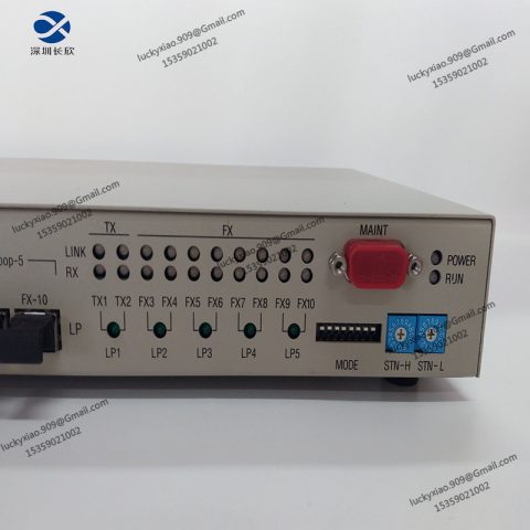
AMAT 0190-26873: Technical Specifications
- Component Type
- Category: Wafer Handling Robot Arm or Precision Motion Stage
- Purpose: Facilitates high-speed, ultra-clean transfer of wafers between chambers in vacuum cluster tools.
- Material: Carbon fiber-reinforced composite (for lightweight rigidity) with ceramic coatings (e.g., Al₂O₃) for particle-free operation.
- Physical Specifications
- Arm Reach: 600–800 mm (optimized for 300mm wafer platforms).
- Payload Capacity: 5–10 kg (supports multiple wafers or process kits).
- Weight: 4.5–6.0 kg (balanced for high acceleration/deceleration).
- Motion & Control
- Speed: Up to 1.5 m/s with positional accuracy of ±0.1 mm.
- Degrees of Freedom: 6-axis control for precise alignment (X, Y, Z, θ, tilt, radial).
- Vacuum Compatibility: Operates in high-vacuum (≤ 10⁻⁷ Torr) and controlled atmospheres (N₂ purge).
- Environmental Tolerance
- Temperature Range: -20°C to 120°C (operational); survives thermal cycling up to 300°C.
- Cleanliness: Class 1 (ISO 14644-1) particle-free performance.
- Integration & Interfaces
- Tool Compatibility: Designed for AMAT Endura® or Centura® platforms.
- Control System: Integrated with SECS/GEM protocols for real-time synchronization with tool automation.
- Sensors: Encoders and laser alignment systems for closed-loop positioning.
- Certifications & Standards
- Compliant with SEMI S2/S12 (safety and contamination control).
- Meets SEMI E178-0315 for robotic accuracy and repeatability.
- Lifetime & Maintenance
- Service Life: 3–5 years (or 1 million transfer cycles), depending on operating intensity.
- Maintenance: Lubrication-free bearings; monthly inspection for wear on gripper pads.
Functional Overview
The AMAT 0190-26873 is critical for high-throughput semiconductor manufacturing, enabling rapid, contamination-free wafer transfers. Key functionalities include:
- High-Speed Wafer Handling
- Transfers wafers between load locks, process chambers, and metrology stations with sub-millisecond synchronization, minimizing cycle time.
- Precision Alignment
- Ensures ±0.05 mm wafer placement accuracy for processes requiring nanoscale overlay (e.g., EUV lithography, atomic layer deposition).
- Ultra-Clean Operation
- Eliminates particle generation through non-shedding materials and electrostatic discharge (ESD)-safe design.
- Flexible Configuration
- Adapts to multi-chamber cluster tools, supporting sequential processes like etch-deposition-clean in a single pump-down.
- Applications
- Advanced Logic/DRAM Fabrication: Transfers wafers in 3nm/5nm node processes.
- 3D NAND Stacking: Handles delicate wafers during high-aspect-ratio via etching.
- Metrology Integration: Positions wafers for inline defect inspection or thickness measurement.
-480x480.jpg)
There are no reviews yet.